Tehnička dokumentacija
Tehnički podaci
Brand
Renesas ElectronicsProduct Type
Clock Buffer
Maximum Input Frequency
200MHz
Maximum Propagation Delay Time
350ps
Mount Type
Surface
Package Type
SOIC
Pin Count
8
Minimum Supply Voltage
3V
Maximum Supply Voltage
4.6V
Minimum Operating Temperature
-40°C
Maximum Operating Temperature
85°C
Standards/Approvals
No
Series
IDT23S05E
Automotive Standard
No
Zemlja podrijetla
Philippines
Detalji o proizvodu
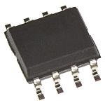
The Renesas Electronics zero delay clock buffer is a high-speed phase-lock loop (PLL) clock buffer, designed to address high-speed clock distribution applications. The zero delay is achieved by aligning the phase between the incoming clock and the output clock, operable within the range of 10 to 200MHz. The PLL feedback is on-chip and is obtained from the CLKOUT pad. In the absence of an input clock, it enters power down.

Zamisliti. Stvoriti. Surađivati
PRIDRUŽITE SE BESPLATNO
Bez skrivenih naknada!


Informacije o stanju skladišta trenutno nisu dostupne.
KM 20,13
KM 2,013 Each (Supplied in a Tube) (bez PDV-a)
KM 23,55
KM 2,355 Each (Supplied in a Tube) (s PDV-om)
Proizvodno pakovanje (cijev)
10
KM 20,13
KM 2,013 Each (Supplied in a Tube) (bez PDV-a)
KM 23,55
KM 2,355 Each (Supplied in a Tube) (s PDV-om)
Informacije o stanju skladišta trenutno nisu dostupne.
Proizvodno pakovanje (cijev)
10
| količina | Jedinična cijena | Po cijev |
|---|---|---|
| 10 - 20 | KM 2,013 | KM 10,07 |
| 25+ | KM 1,969 | KM 9,84 |
Zamisliti. Stvoriti. Surađivati
PRIDRUŽITE SE BESPLATNO
Bez skrivenih naknada!
Tehnička dokumentacija
Tehnički podaci
Brand
Renesas ElectronicsProduct Type
Clock Buffer
Maximum Input Frequency
200MHz
Maximum Propagation Delay Time
350ps
Mount Type
Surface
Package Type
SOIC
Pin Count
8
Minimum Supply Voltage
3V
Maximum Supply Voltage
4.6V
Minimum Operating Temperature
-40°C
Maximum Operating Temperature
85°C
Standards/Approvals
No
Series
IDT23S05E
Automotive Standard
No
Zemlja podrijetla
Philippines
Detalji o proizvodu
The Renesas Electronics zero delay clock buffer is a high-speed phase-lock loop (PLL) clock buffer, designed to address high-speed clock distribution applications. The zero delay is achieved by aligning the phase between the incoming clock and the output clock, operable within the range of 10 to 200MHz. The PLL feedback is on-chip and is obtained from the CLKOUT pad. In the absence of an input clock, it enters power down.
Zamisliti. Stvoriti. Surađivati
PRIDRUŽITE SE BESPLATNO
Bez skrivenih naknada!